If you feel unsure about these prerequisites, please read the prelab material carefully.
The goal of this lab is to build some simple TTL circuits[1] to enhance your understanding of Boolean algebra.
Logic gates can perform basic Boolean operations like AND, OR, and NOT. Also, logic gates that implement more advanced Boolean operations like NAND, NOR, XOR, and XNOR are available.
In most applications, NAND gates and NOR gates are the most commonly used, because they use less transistors internally than other types of gates do, which makes them cheaper to produce and buy. Also, NAND gates can actually be used to build any type of Boolean operator we need.
Here are some pin diagrams for chips in the 7400 series (the series that we are using in class). These diagrams show you which pins on the chips correspond to which portion of a particular gate (each chip has multiple gates on it).
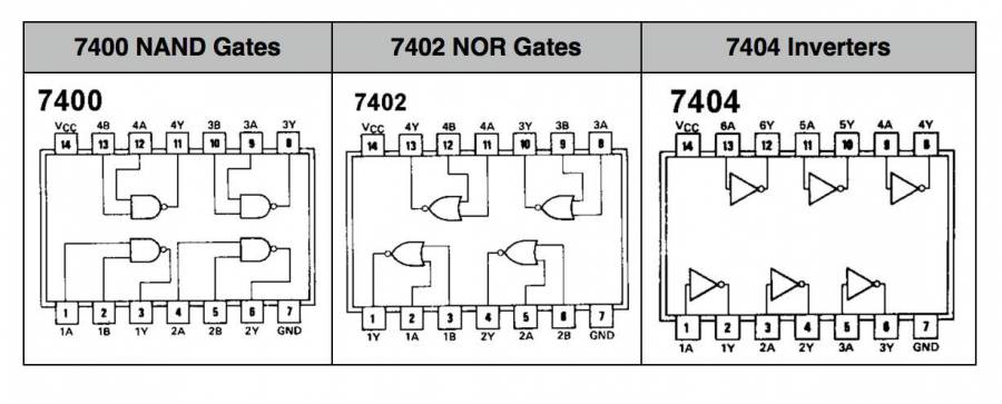
Make sure you can read the print on the chip when referencing the diagram: if the part number on the chip is upside down, then you are holding the chip upside down.
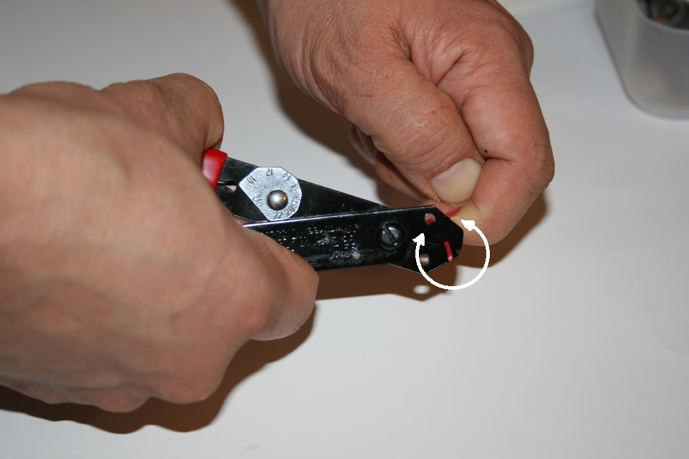
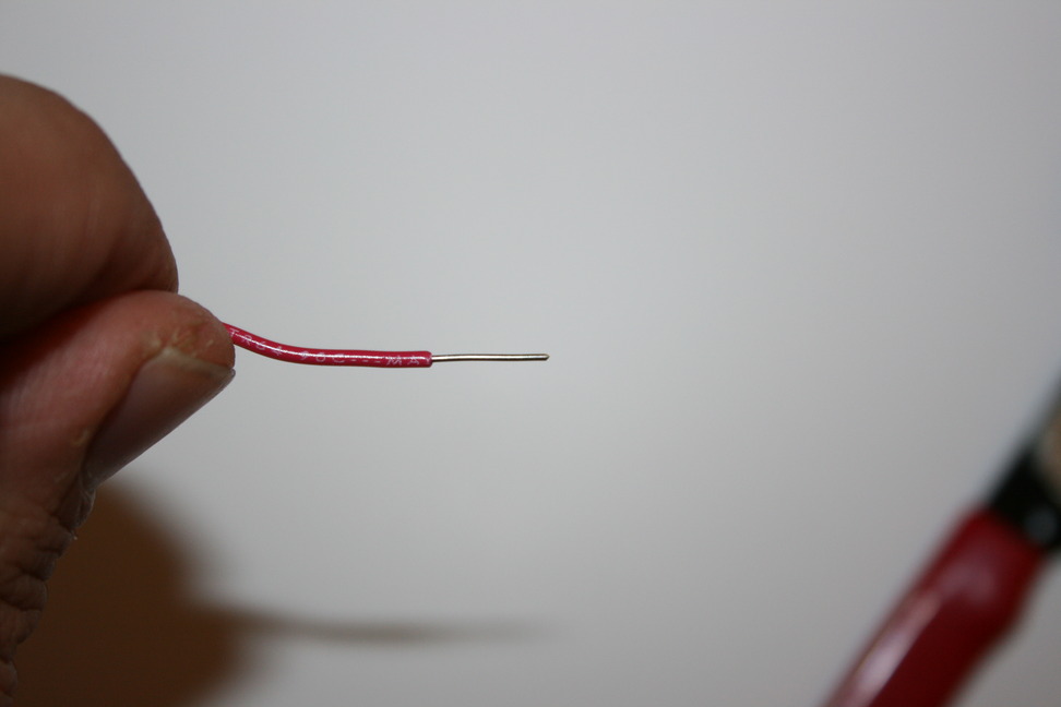
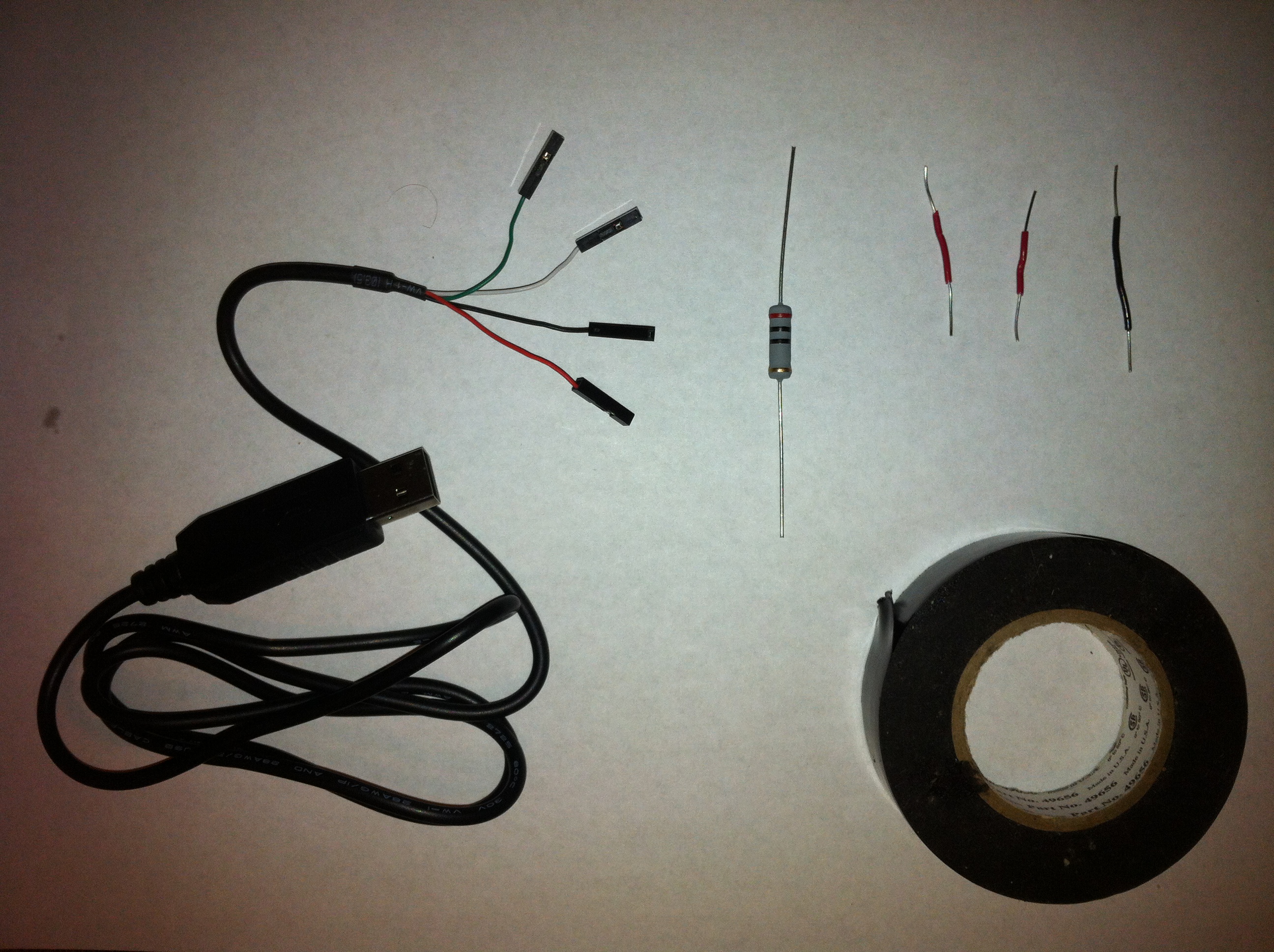
Use the cutter at the base of the pliers to cut the wire. To strip the plastic from the conductor select the 22AWG knob in the tool and press the wire with the hole at the top of the tool. Rotate the tool around the wire to cut the plastic and then pull out toward the end of the wire. If you need to put too much force to pull the plastic out, try rotating the tool 360° to cut the plastic first. The kit includes wire of different colors and wire strippers. You will use the wire strippers provided in the lab to cut the wires and remove the plastic from the conductor. Leave about 1/4 inch of conductor in each side.
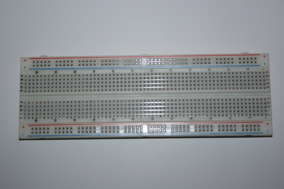
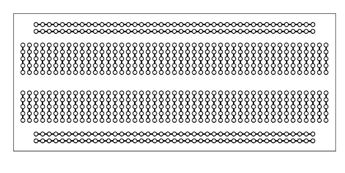
The breadboard is a base made of a matrix of sockets used to build temporal electronic circuits. Here is the picture of the breadboard you will use in this lab.
In the breadboard, the 2 top and 2 bottom rows are used for the power. The columns in the middle are connected according to the following picture.

These little switches are 1/4” on each side, cost about 25 cents, and can plug directly into a breadboard. These mechanical devices have 4 legs, which may make you think that there are 4 wires that are switched on and off, but in fact, two on each side are actually connected together inside. So really, this switch is just a 2-wire switch.
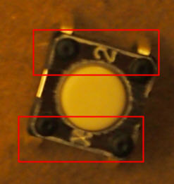
Normally, the two wires with a label on their side are disconnected (normally open) but when you press the little button on top, they are mechanically connected.
To get the buttons to sit better in the breadboard, you may want to straighten out the legs (just squish them with a pair of pliers) so that they look like the button on the above.
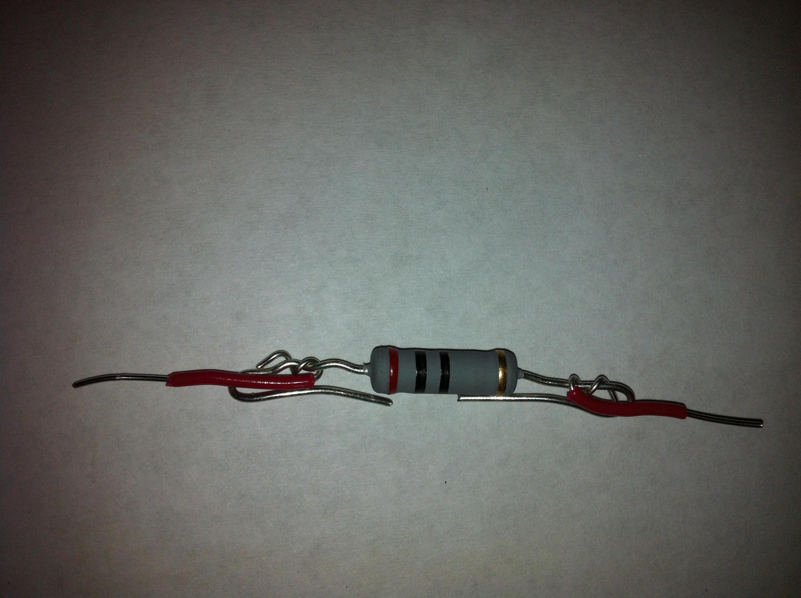
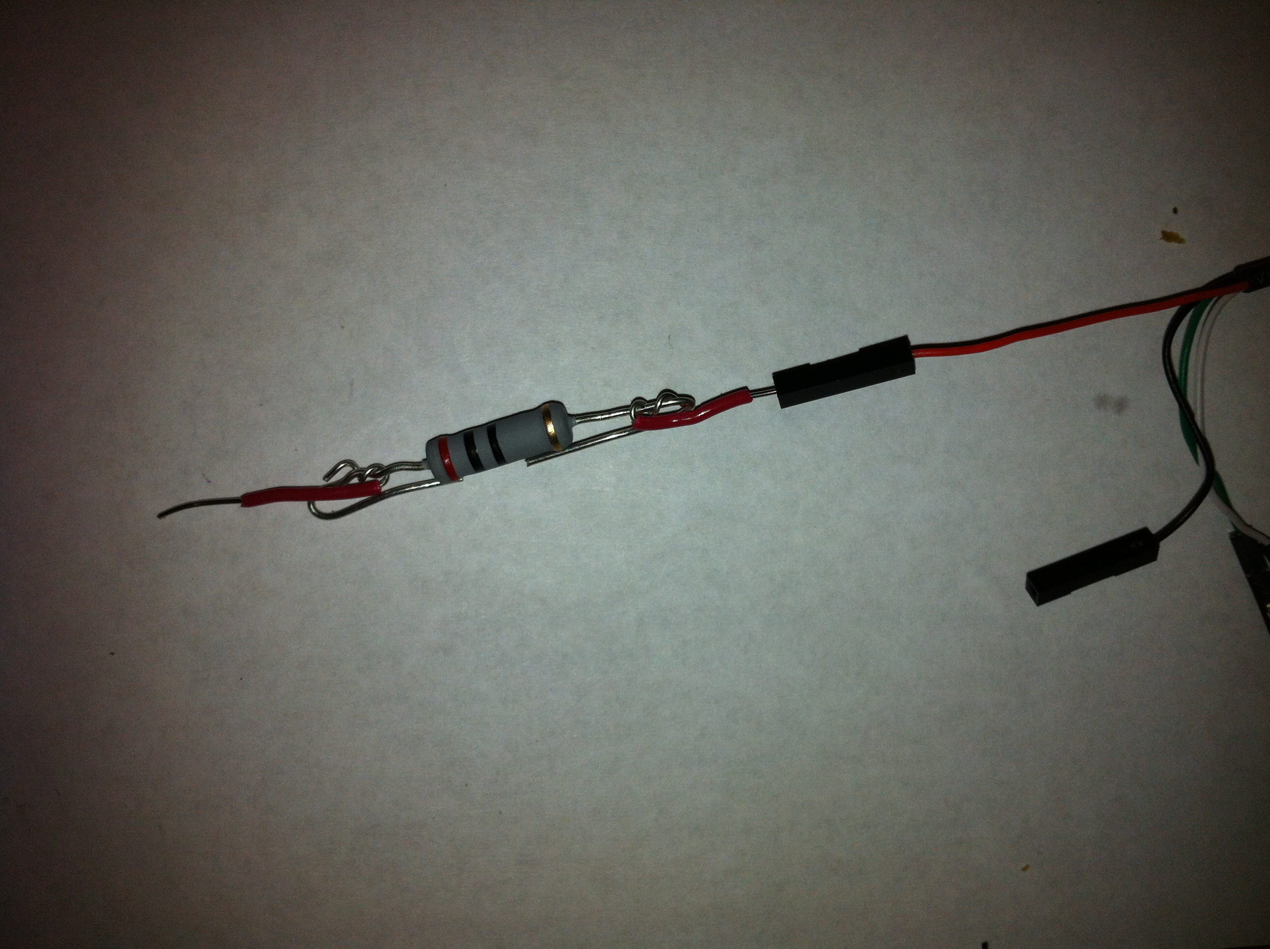
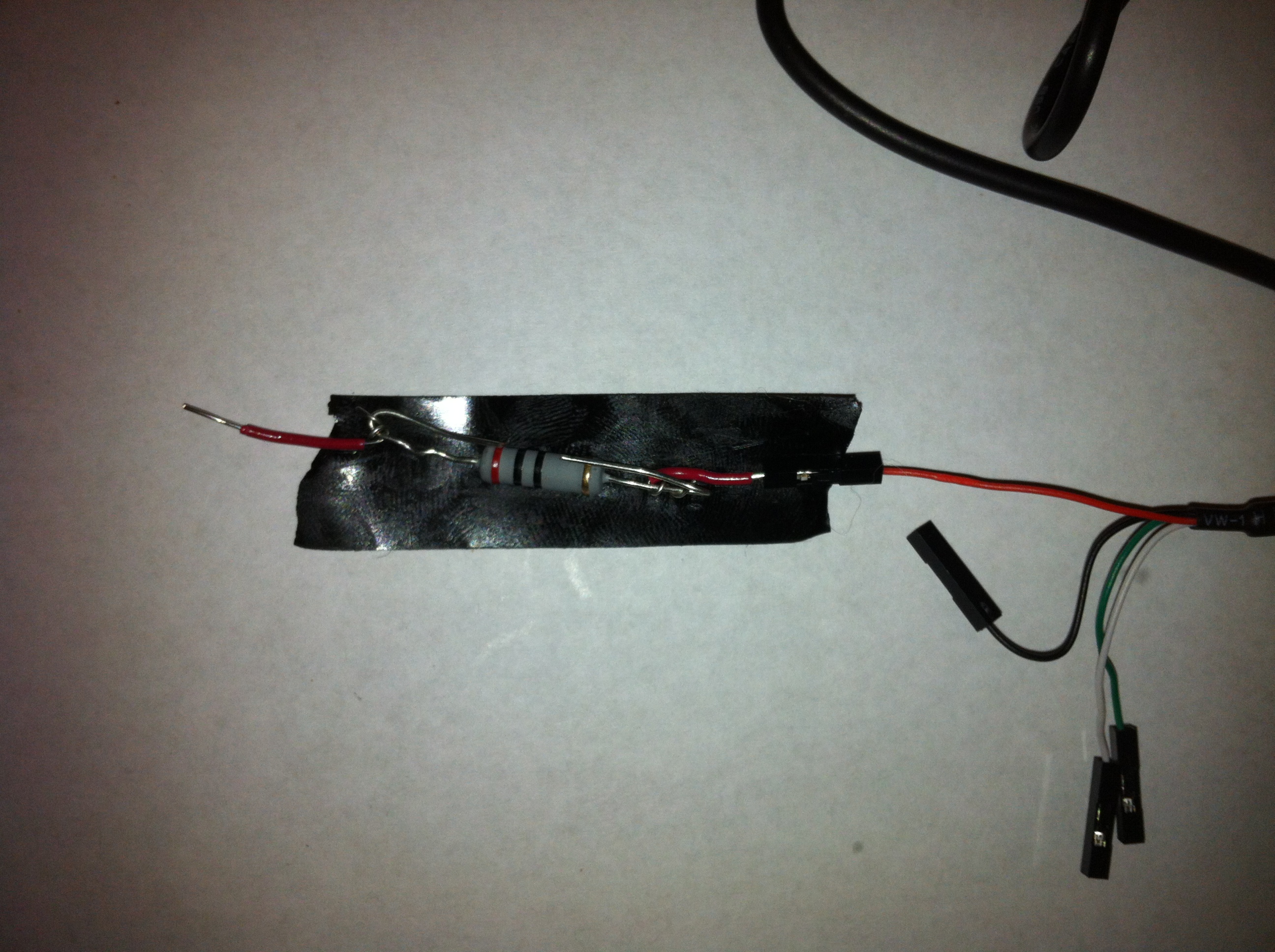
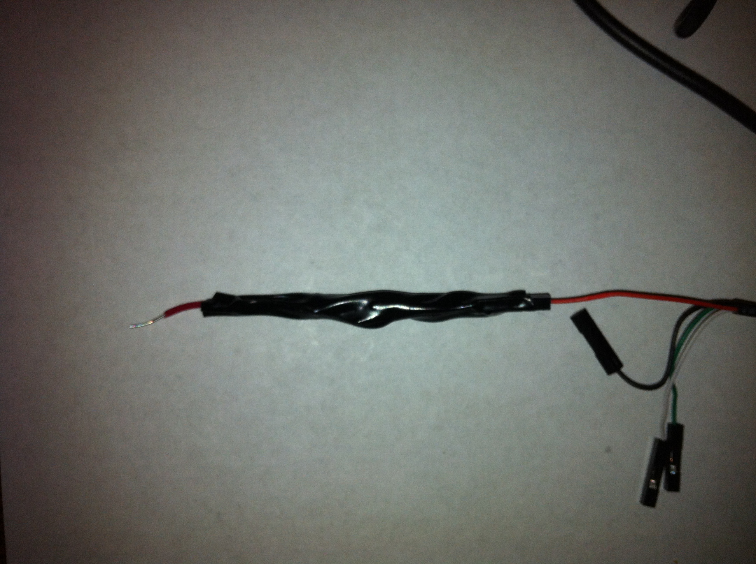
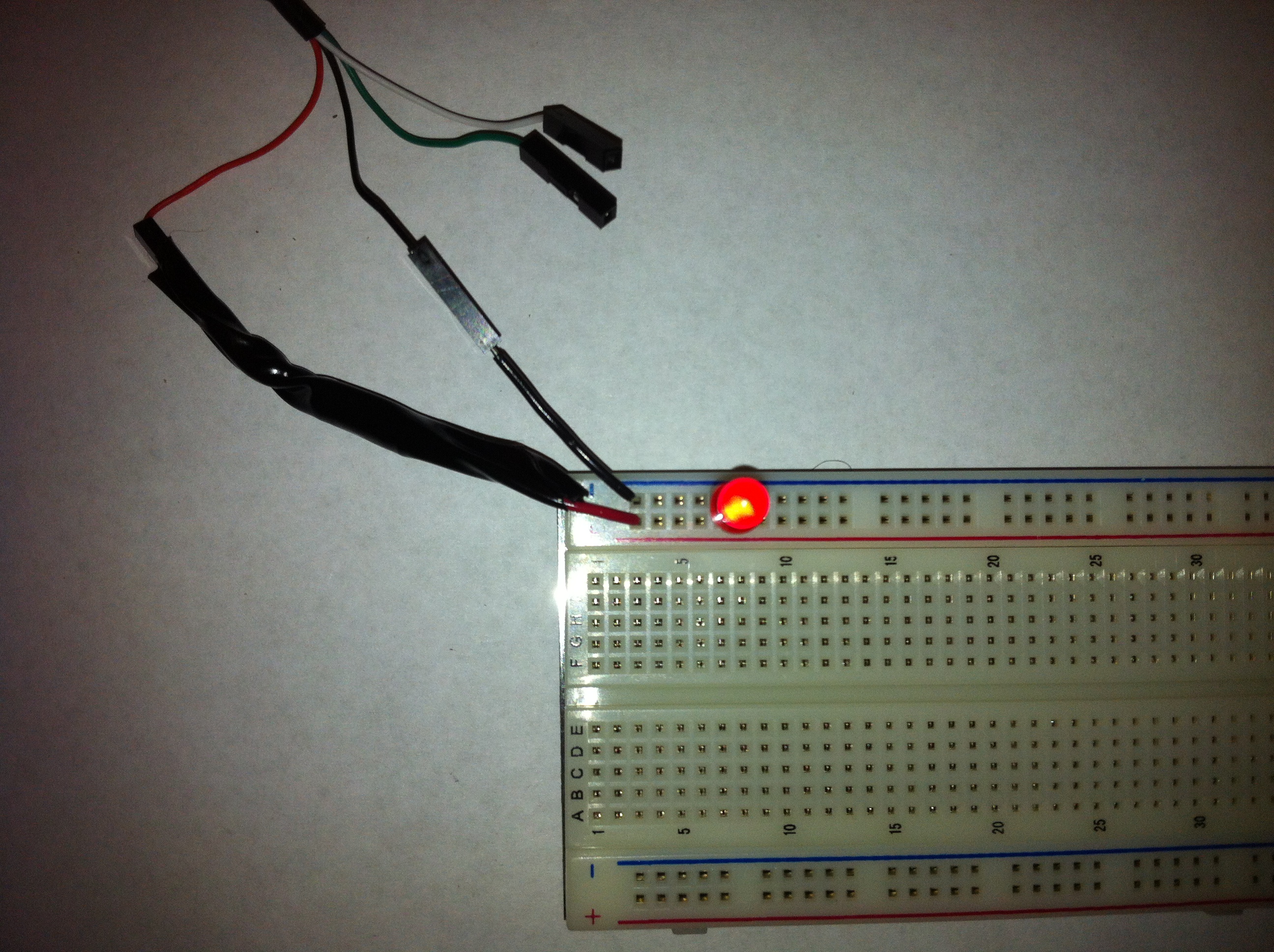
In the hardware labs, we are going to use the USB-TTY cable to connect to the computer. To prevent a short circuit, we will first connect the cable with a resistor (usually 20 ohms). We will then connect the red and black wires to the positive and negative rows on your breadboard, respectively. You should also do this simply to test whether the USB to TTY cable works or not.
You will need to cut two 1-inch red wires and one 2-inch black wire and strip the plastic from the ends. Also you will need about 4 inches of electric tape.
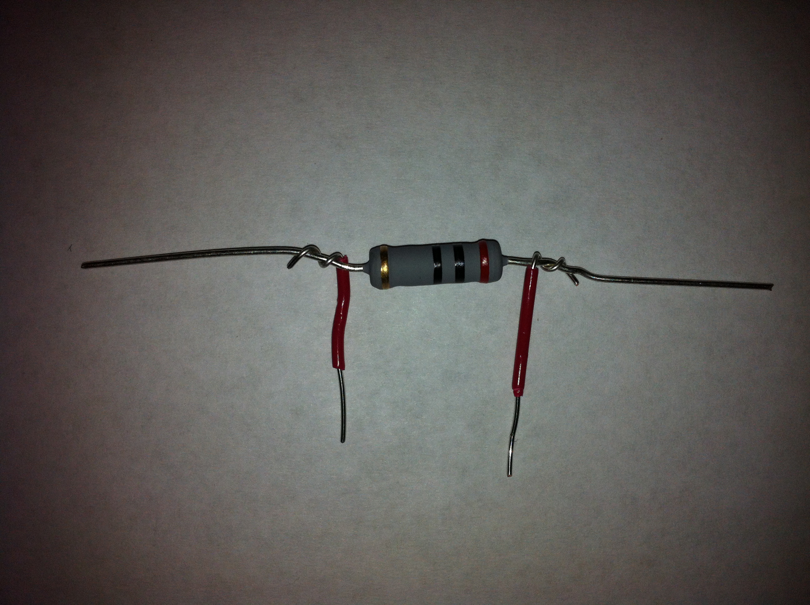
The 20-ohm resistor (red-black-black) is provided in the kit.
IMPORTANT: Do not directly connect the USB-TTY cable to the resistor, because the resistor terminals are thicker than the USB-TTY cable terminals, and this will damage the terminal.
In this part, you are going to implement a XNOR gate with 5 NAND gates. You are not allowed to use any gates except NAND gates.
Recall that for Boolean variables A and B, A XNOR B is true when A and B are both true or both false. Otherwise A XNOR B is false.
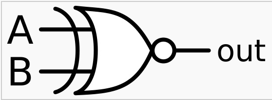
Thus, the truth table of the XNOR gate is:
| A | B | A XNOR B |
| 0 | 0 | 1 |
| 0 | 1 | 0 |
| 1 | 0 | 0 |
| 1 | 1 | 1 |
In order to implement XNOR using NAND gates, we need to first get an expression for XNOR in terms of NANDs. We can obtain a trivial expression for A XNOR B in terms of AND and OR by looking at the truth table: since A XNOR B is true when both A and B are 0 or both A and B are 1, then we have that A XNOR B = AB + A'B'.
| AB + A'B' | = [(AB + A'B')']' | Double Negation |
| = [(AB)'(A'B')']' | De Morgan's Law | = [(A NAND B)(A' NAND B')]' | (AB)' = A NAND B | = (A NAND B) NAND (A' NAND B') | (AB)' = A NAND B |
Now you are almost done. The only thing that remains is to remove NOTs from the expression.
Note that A' = A NAND A and B' = B NAND B.Write down this result.
Now that you have your Boolean expression for A XNOR B in terms of NANDs, draw out a circuit diagram of how the circuit should look.
A common mistake that students make is to forget to power their circuit component. Make sure you remember to supply power and ground to your NAND chips according to their pin diagram.
Another important thing you should remember is to always put a resistor in your circuit. This resistor is usually called the protecting resistor, because it reduces the current to minimize the chances of burning out your chip.
For this part, we will provide a circuit diagram for you, since this is your first time designing a circuit.
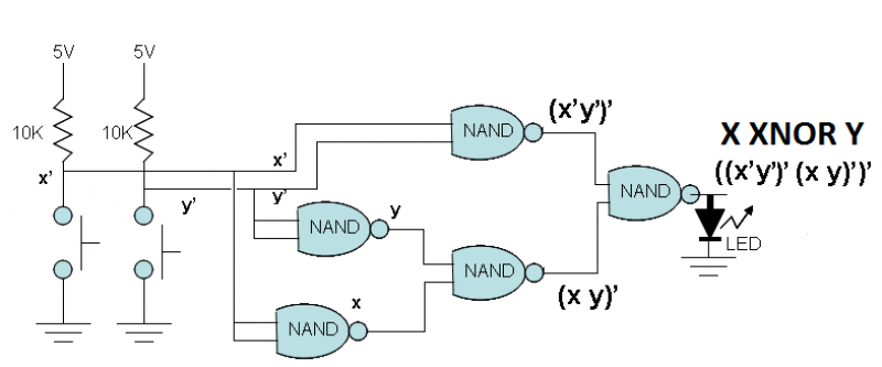
Note how we show not just the NAND gates in the diagram, but also the switches, power and ground.
The following is a step-by-step guide to implementing the circuit we designed above. This may be your first electrical lab experience, so be careful!
One important tip is to make sure to plan the wiring of your circuit carefully, as a very messy circuit with errors is extremely difficult to debug.
Notice that the NAND chips are the ones labeled SN74HCT00N. .
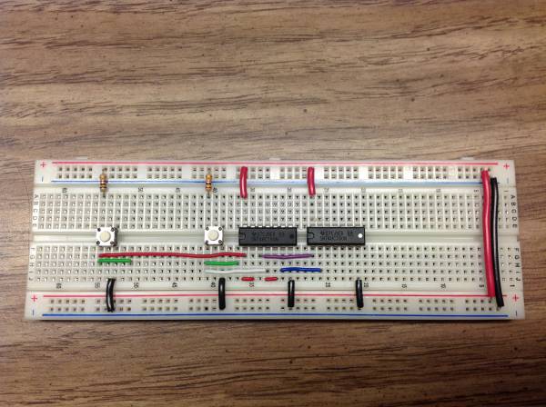
One other thing to note is that when the switch is wired so that resistor goes to +5V, the terminal of the push button produces a 1 when not pushed and 0 when pushed. Also, you can test your circuit step by step.
Step 1.
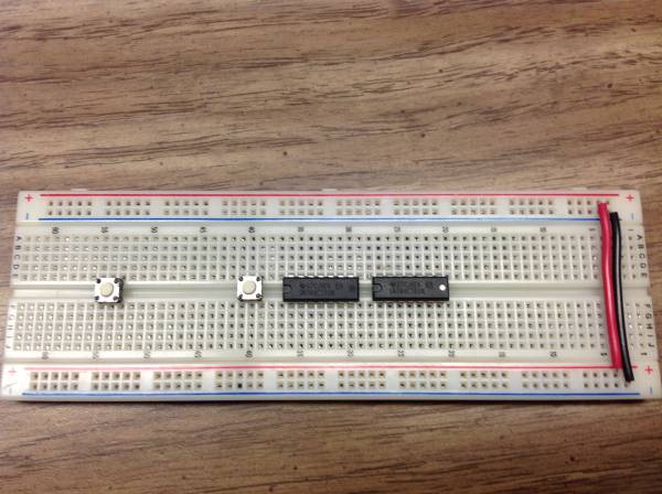
Step 2.
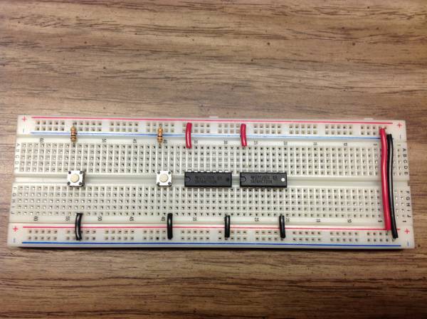
Step 3.
Step 4.
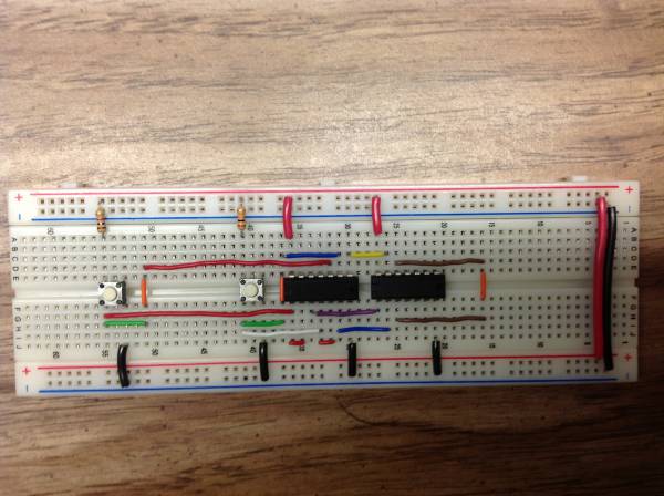
Don't forget to provide a power source to your circuit. Your circuit needs a power supply to work.
Check your circuit carefully before your turn on the power source. Make sure there is no short circuit.
Step 5.
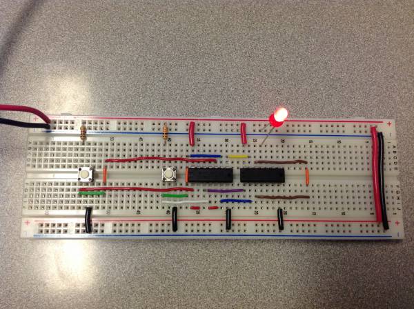
Check your circuit. If you have wired everything correctly, the output LED will be ON when the state of both buttons is the same (both are pressed/not pressed) and the LED will be OFF when the state is different (one button is pressed and the other released).
Sometimes you might connect a wire to the wrong pin. Use the pin diagrams provided above as a reference.
In this take-home portion of this lab, you are going to implement a three-input NAND gate. The three-input NAND gate works similarly to a regular two-input NAND gate - assuming your 3 inputs are A, B and C, the result should be the negation of A AND B AND C. You should first fill in the following truth table:
| A | B | C | Out |
| 0 | 0 | 0 | 1 |
| 0 | 0 | 1 | 1 |
| 0 | 1 | 0 | 1 |
| 0 | 1 | 1 | 1 |
| 1 | 0 | 0 | |
| 1 | 0 | 1 | |
| 1 | 1 | 0 | |
| 1 | 1 | 1 |
HINT: A three-input NAND gates is not simply a combination of two NAND gates.
You should use three push buttons as inputs and a LED to show your output.
Next lab session, you should bring your circuit and show how it works to your PSO TA.
The take-home portion is due at the beginning of the first lab sessionext week.
[1]: In the early ages of computing, Before integrated chips (or ICs) were invented, vacuum tubes were used to build vast circuits inside computers. These tube-based computers were enormous, and the vacuum tubes used in them frequently burnt out, so scientists and engineers worked on a replacement for the unwieldy tubes. The replacement they came up with was the transistor.
TTL stands for Transistor-Transistor Logic. The digital circuits we use today are built from bipolar junction transistors and resistors. We call these circuits TTL circuits because transistors can perform Boolean operations.