The NAND flash of a solid-state drive stores data differently. Recall that NAND flash has transistors arranged in a grid with columns and rows. If a chain of transistors conducts current, it has the value of 1. If it doesn't conduct current, it's 0. At first, all transistors are set to 1. But when a save operation begins, current is blocked to some transistors, turning them to 0. This occurs because of how transistors are arranged. At each intersection of column and row, two transistors form a cell. One of the transistors is known as a control gate, the other as a floating gate. When current reaches the control gate, electrons flow onto the floating gate, creating a net positive charge that interrupts current flow. By applying precise voltages to the transistors, a unique pattern of 1s and 0s emerges.
NAND flash comes in two flavors based on how many 1s and 0s can be stored in each cell. Single-level cell (SLC) NAND stores one bit -- either a 1 or a 0 -- per cell. Multi-level cell (MLC) NAND stores two bits per cell. MLC flash delivers higher capacity, but it wears out more quickly (yes, wears out -- we'll cover that more in a couple of pages). Still, it's less expensive per gigabyte than SLC and, as a result, is the preferred technology in almost all consumer-level SSDs.
Cost has been one of the biggest hurdles of flash memory and, consequently, of solid-state drives. But in recent years, costs have dropped significantly. At the same time, advances in NAND flash development have taken what's good about the technology and made it even better. Up next, we'll look at the advantages of solid-state drives.
Solid-state drives are called that specifically because they don’t rely on moving parts or spinning disks. Instead, data is saved to a pool of NAND flash. NAND itself is made up of what are called floating gate transistors. Unlike the transistor designs used in DRAM, which must be refreshed multiple times per second, NAND flash is designed to retain its charge state even when not powered up. This makes NAND a type of non-volatile memory.
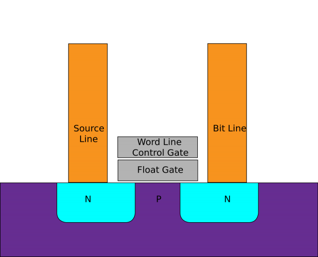
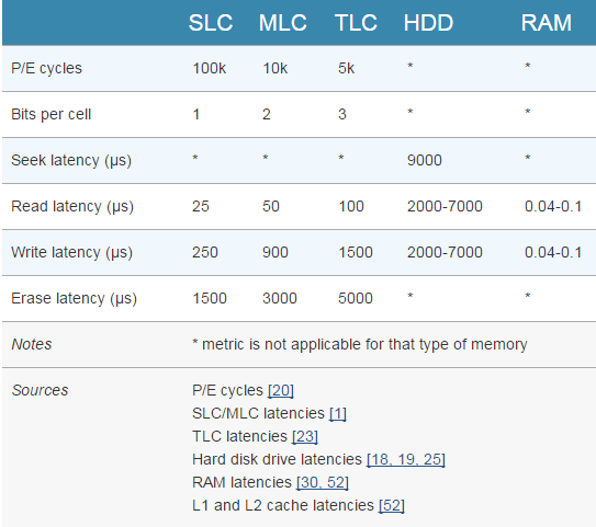
The diagram above shows a simple flash cell design. Electrons are stored in the floating gate, which then reads as charged “0” or not-charged “1.” Yes, in NAND flash, a 0 means data is stored in a cell — it’s the opposite of how we typically think of a zero or one. NAND flash is organized in a grid. The entire grid layout is referred to as a block, while the individual rows that make up the grid are called a page. Common page sizes are 2K, 4K, 8K, or 16K, with 128 to 256 pages per block. Block size therefore typically varies between 256KB and 4MB. One advantage of this system should be immediately obvious. Because SSDs have no moving parts, they can operate at speeds far above those of a typical HDD. The following chart shows the access latency for typical storage mediums given in microseconds.
NAND is nowhere near as fast as main memory, but it’s multiple orders of magnitude faster than a hard drive. While write latencies are significantly slower for NAND flash than read latencies, they still outstrip traditional spinning media. There are two things to notice in the above chart. First, note how adding more bits per cell of NAND has a significant impact on the memory’s performance. It’s worse for writes as opposed to reads — typical triple-level-cell (TLC) latency is 4x worse compared with single-level cell (SLC) NAND for reads, but 6x worse for writes. Erase latencies are also significantly impacted. The impact isn’t proportional, either — TLC NAND is nearly twice as slow as MLC NAND, despite holding just 50% more data (three bits per cell, instead of two).
Source: How stuff works